Reading noteFrom PCIe(四)—— 物理层
PCIe, part 4: the physical layer (1)
The PHY layer is where it starts to hurt.
The PHY layer
In the PCIe spec the physical layer is presented as two separate parts: the physical layer logical sub-block and the physical layer electrical sub-block, the latter normally built out of a SerDes.
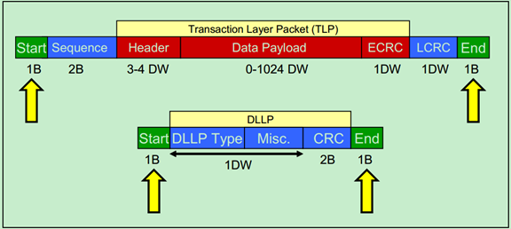
The PHY sits at the very bottom of the PCIe architecture, so both TLPs and DLLPs have to go through it to be transmitted and received. TLPs and DLLPs coming down from the data link layer are held temporarily in the physical layer’s buffer and get start and end characters added; these are sometimes also called frame characters.
TLP and DLLP here refer to who originally sent the packet: a TLP is a packet whose original sender was the transaction layer, a DLLP one whose original sender was the data link layer. But a TLP still passes through the data link layer, which adds the sequence number and LCRC.
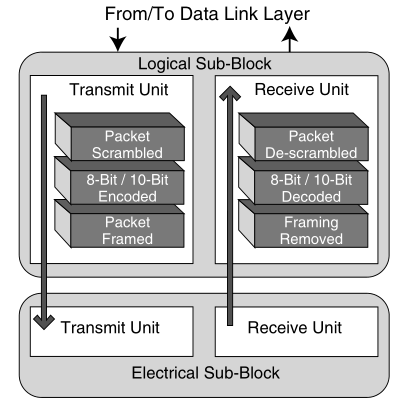
The PCIe PHY layer splits into two sub-blocks:
- The logical sub-block
- Encoding and decoding:
- Data integrity: the logical sub-block uses advanced coding techniques (8b/10b encoding, or 128b/130b encoding) to strengthen the integrity of the transfer. That coding helps the receiver correctly detect and correct possible errors, and is indispensable at high speed.
- Bandwidth optimisation: appropriate coding can reduce the signal bandwidth needed, optimising overall system performance by lowering the bit error rate.
- Clock recovery and data synchronisation:
- Clock management: with no separate clock line, the logical sub-block has to recover the clock from the incoming data signal, which is one of the technical challenges of high-speed serial communication. Clock recovery is what makes the data get sampled at the right moment, reducing timing errors.
- Alignment and synchronisation of the data stream: the logical sub-block is also responsible for aligning the data stream, so packets are handled correctly at the link layer. That means handling any bit-shift errors or timing skew in the stream, which is essential to keeping the data accurate and consistent.
- Encoding and decoding:
- The electrical sub-block
- Transmission: the electrical sub-block turns the data encoded by the logical sub-block into electrical signals and sends them over the physical medium (a cable, or the traces on a board). This is the digital-to-analogue step, and it is what makes transmission at the physical layer reliable.
- Reception and conversion: at the receiving end, the electrical sub-block turns the electrical signals coming off the physical medium back into digital encoded data, which it then passes up to the logical sub-block to be decoded.
- Handling the electrical characteristics: the electrical sub-block also deals with the electrical properties of the physical link — level adjustment (keeping the signal within the right voltage range), differential signalling (using two signals at opposite levels to reduce noise), and so on.
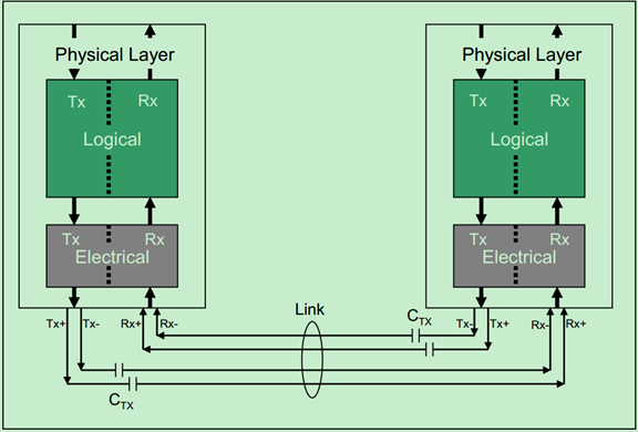
As the figure above shows, the PCIe physical layer implements a transmit and a receive differential pair, so communication is full duplex. Note that the PCIe spec only specifies what the physical layer has to do, how well, and to what parameters — it does not state how to implement any of it. In other words, a vendor can design its PCIe physical layer to suit its own needs and circumstances. What follows uses the example from the Mindshare book to sketch the logical part of the PCIe physical layer. It may differ from how other vendors’ devices implement it, but the design goals and the eventual function are basically the same.
The character of PCIe signalling is high frequency and short distance, and all of this is designed to help transmit such signals stably. The main design goals are:
- DC balance
- Definition and purpose: DC balance means keeping the number of logic “0”s and “1”s in the transmitted data roughly equal. This reduces the signal’s DC bias, helps keep the voltage in the circuit balanced, and avoids a long-term drift in the signal level.
- How it is done: DC balance is achieved by using a particular coding scheme, such as 8b/10b or 128b/130b. These schemes not only balance the data bits against each other but also add extra control bits that help monitor and maintain the overall quality of the signal.
- Stable transmission at high frequency
-
Purpose
: several potential problems have to be solved to transmit data stably at high frequency:
- Signal distortion: at high frequency, if the level cannot rise and fall fast enough, the shape of the signal may be distorted, affecting how accurately the data is read.
- Jitter: the timing of the signal on the transmission line varies, possibly because of line quality or external interference, which affects the timing accuracy of the signal.
- Filter problems: a long run of identical bits may keep the signal from passing through the receiver’s filter properly, which is why a specific coding technique is needed to avoid long runs of the same bit.
-
How it is done: use differential signalling (PCIe’s main physical interface is a differential pair). Carrying two signals of opposite polarity on two lines greatly reduces the effect of external noise and improves signal integrity.
- Minimising EMI (electromagnetic interference)
- Purpose: at high frequency, a repeating data pattern easily produces electromagnetic interference, which disturbs the equipment around it. PCIe devices also need to resist interference coming from other devices.
- How it is done: shielding and careful layout, to reduce both the generation and the effect of EMI. Coding techniques (such as the DC-balancing codes above) also help, by breaking up data sequences that could form a repeating pattern, which lowers the EMI risk.
Let’s go through the physical layer design piece by piece.
The physical layer also handles a number of other things, such as link initialisation, data rate negotiation, and plenty more. They have little to do with the main thread here — moving data — so they are not covered; look them up if you need them.
Links and lanes
Not important to the design; this is the physical connector.
Before getting into the detail of the physical layer, let’s look at what PCIe actually looks like physically, and at the concepts of link and lane.
You have seen PCIe slots on a motherboard. The shortest is PCIe x1, which is rarely used; the longest is PCIe x16, which takes a graphics card. There is also an x32 slot, but only in large servers. As shown here: https://www.ccboot.com/correct-pcie-slot.htm
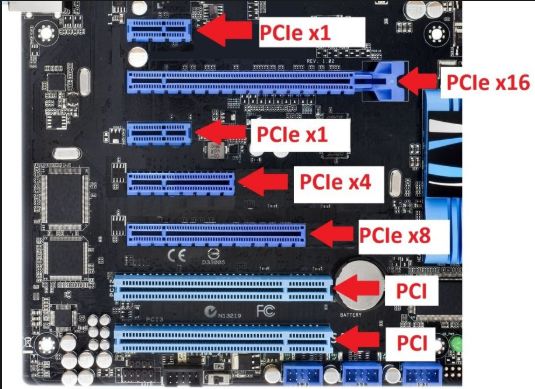
Multiple lanes, one link
- Lane:
- In the PCIe architecture, a lane is made of two differential pairs, one for transmit and one for receive. Each differential pair is two wires: one for the positive signal, one for the negative. This arrangement helps reduce noise and improve signal integrity.
- A 16-lane (x16) PCIe device therefore has 16 such differential pairs, that is, 32 physical wires.
- Link:
- A link is a collection of lanes, used to connect two PCIe devices. Although an x16 link has 16 lanes, those lanes all work together on the same transfer, serving a single device.
- Data travels over the link in parallel across multiple lanes at once, but within each lane the data is serial. The data is split into pieces, each piece sent serially over one lane, which raises the overall transfer rate substantially.
- Recombining the data:
- At the receiving end, the data from all the lanes is recombined into the original data stream. This keeps the transfer efficient while preserving the data’s integrity and order.
Slot compatibility and the mechanical key
- Slot design:
- PCIe slots are designed so that cards of different lengths fit into slots of the corresponding length. A short card with fewer lanes (an x1, x4 or x8 card) can be plugged into an x16 slot, thanks to PCIe’s flexible, backwards-compatible design.
- The pins in a slot are divided into two parts: the common part and the part dedicated to data lanes. The common part carries power, ground and some necessary control signals.
- Mechanical key:
- The mechanical key is a physical feature of the slot, a small divider, which prevents the wrong type of card being plugged into an incompatible slot. It ensures physical compatibility and also avoids potential electrical faults.
- The key’s position and shape vary by slot type (x1, x4, x8, x16), which helps the user tell them apart and install a PCIe card correctly.
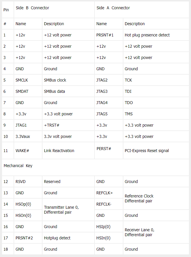
The PCIe slot’s pin arrangement is carefully allocated, which is what lets one slot design support anything from x1 to x16 while staying compatible and flexible. Here is a closer look at the “common part” and the “data lanes” of a PCIe slot, and how they support different devices and interoperation.
The common part
The common part sits at the front of the PCIe slot, and its pinout is the same whatever the slot size (x1, x4, x8, x16). It covers these main functions:
-
Power:
- It supplies plenty of 12 V and 3.3 V inputs and grounds. Spreading the current across several contacts avoids overloading any one of them and keeps the device running stably.
-
JTAG debug interface:
- JTAG is used to test, monitor and debug the board. It is an important tool for engineers finding problems, validating designs and testing hardware performance during design and production.
-
SMBus (System Management Bus):
- SMBus carries device information, such as sensor data. It lets the system read key parameters such as temperature and voltage, for monitoring and management.
-
WAKE# and PREST# pins:
- WAKE# wakes the device from a low-power state.
- PREST# is a hardware reset, which is useful when the system needs to restart quickly or return to normal operation.
The data lanes
The data lanes are at the back of the slot, separated by the mechanical key (a physical divider). How many of these pins there are, and how they are arranged, depends on the slot type (x1, x4, x8, x16). The data lanes include:
-
Grounds:
- Each functional pin has ground pins on both sides, which helps keep the signal clean and reduces crosstalk and EMI.
-
Clock lines:
- Supply the clock signal used to synchronise the transfer.
-
Transmit and receive lanes:
- These carry data out and in respectively. In an x16 configuration there are 16 times as many of them as in x1, which gives a much higher transfer rate.
-
Hot-plug detect pins:
- Detect the card being inserted or removed, so a device can be hot-plugged safely — plugged in or pulled out without powering down.
The “magic” of scaling
PCIe is designed so the physical layer adapts to cards of different sizes by detecting how many lanes are in use. An x1 card can go into a slot of any size (x1, x4, x8, x16), because all of those slots have the same common part and at least one complete set of data lane pins. This design greatly improves the interoperability of PCIe devices and the flexibility of the system.
In this way PCIe not only makes data transfer between hardware efficient, but also gives the system design a high degree of compatibility and room to grow, so users and system designers can upgrade or swap hardware as they need to.
The logical sub-block
When the data link layer passes the packaged data down, the first thing it reaches is the logical sub-block. Here we do some processing on the data: scrambling, encoding, inserting control characters, and so on.
Link serialisation
Here we can see how a PCIe packet is spread across an x4 link. The figure shows how a Transaction Layer Packet (TLP) is split up and transmitted over several lanes. In detail:
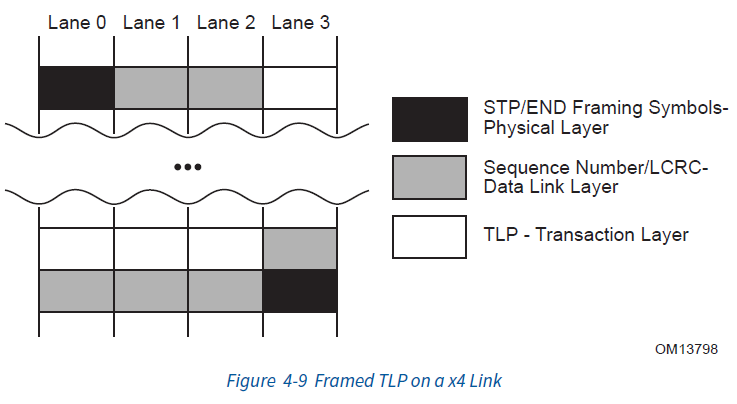
Distributing the data across the link
- What the packet contains:
- TLP: the transaction layer’s packet, containing the actual data or command to be transmitted.
- Sequence number / LCRC: the data link layer adds a sequence number to each TLP, to guarantee the packet’s integrity and correct ordering. The LCRC (Link CRC) is an error-detecting code used to find errors that occurred in transit.
- STP/END (Start of Packet / End of Packet): the physical layer’s framing symbols, marking the start and end of the packet.
- Distributing across the lanes:
- On the transmit side, the data link layer splits a larger packet (a TLP) into several smaller fragments.
- Those fragments are distributed evenly across the lanes, according to how many lanes the link has (four in this example).
- The physical layer then serialises those fragments, that is, turns them into a serial bit stream to be sent over the lane.
Recombining the data at the receiver
- Reception:
- At the receiver, the physical layer first deserialises the serial bit stream on each lane back into data fragments.
- The data link layer then uses the sequence number and LCRC in the fragments to check the data’s integrity and reassemble the fragments back into the original TLP.
- Processing:
- Once the TLP has been fully reassembled, it is passed up for further processing. A read or write request goes to the appropriate target, for example, and received data may go to the processor or to memory.
This process is what lets PCIe use all the lanes on an x4 link efficiently, raising bandwidth and throughput. Serial transmission on each lane is what allows the signal to be carried accurately at high speed, while the lanes working in parallel greatly improves overall performance. This design is why PCIe can support configurations from x1 to x16, giving it flexibility and headroom across a wide range of applications and requirements.
Data scrambling
Scrambling is a technique commonly used in communication systems. Its purpose is to break up the original order of the data and turn it into what looks like a random sequence, in order to improve the spectral characteristics of the transmitted signal. The process is like a pseudo-random number generator, in that it turns a regular data stream into something that looks like random numbers. With this technique a communication system can improve transmission quality, reduce interference, and make better use of the spectrum. Scrambling is not just a way of improving transmission; it is also a necessary step in meeting particular communication standards and requirements.
What scrambling is for, and how it works
- Avoiding concentrated energy: in digital communication, if the data being transmitted has some regularity or repetition (a run of 0s or 1s, say), the signal’s spectrum ends up with its energy concentrated at certain frequencies. Concentrated energy increases electromagnetic interference (EMI), which is bad for the system.
- Flattening the spectrum: scrambling breaks up the regularity of the data, so the resulting signal is spread more evenly across the spectrum. When the data is in a more random form, the spectrum obtained from its Fourier transform is more uniform, which lowers the energy peaks at particular frequencies.
- Better channel utilisation: by making the signal’s spectrum more uniform, scrambling helps the system use the channel more effectively, because it reduces the non-linear channel effects — interference and distortion — that a concentrated spectrum can cause.
How scrambling is implemented
In a real digital communication system, scrambling is usually implemented with a linear feedback shift register (LFSR), which generates a sequence that looks random and is XORed with the original data to produce the scrambled data. The scrambled data carries less periodicity and regularity in transit, so the signal is more uniform across the whole transmission band.
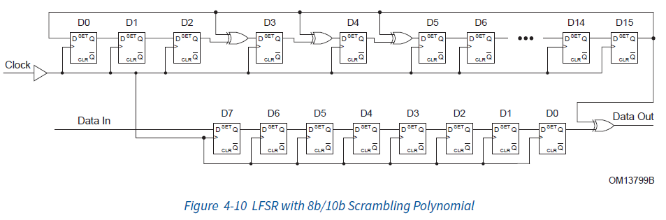
The 16-bit LFSR polynomial for PCIe 1.0 and 2.0
If PCIe 1.0 and 2.0 use a 16-bit LFSR, the polynomial is normally written like this (assuming one of the common polynomials): $$ f(x) = x^{16} + x^5 + x^4 + x^3 + 1 $$ The 23-bit LFSR polynomial for PCIe 3.0 and later
For PCIe 3.0 and later, if a longer 23-bit LFSR is used, the polynomial might be written like this (assuming one of the common polynomials): $$ f(x) = x^{23} + x^{21} + x^{16} + x^{8} + x^{5} + x^{2} + 1 $$
LFSR — write a new post explaining this in detail.
Video explanation: https://www.bilibili.com/video/BV1kA411f76v/?vd_source=480dd1a439e1115a7b44c747b41734f4
The calculation, animated:

So on every clock the LFSR produces one pseudo-random bit, and XORing that bit with the data scrambles it.
One more thing: in PCIe 1.0 and 2.0 the seed of the scrambling LFSR is 0xFFFF, but from PCIe 3.0 on, to avoid similar data appearing on different lanes, each lane’s LFSR has a different seed (lane IDs of 8 and above are taken modulo 8):
| Lane | Seed |
|---|---|
| 0 | 1DBFBCh |
| 1 | 0607BBh |
| 2 | 1EC760h |
| 3 | 18C0DBh |
| 4 | 010F12h |
| 5 | 19CFC9h |
| 6 | 0277CEh |
| 7 | 1BB807h |
The clever part of this approach is that the pseudo-random number produced by the XOR is recoverable: as long as the operand is the same, two XOR operations cancel out. So as long as transmitter and receiver use the same seed, the receiver can run exactly the same LFSR and recover the original data.
Finally, scrambling can be turned off, to make debugging with a scope easier.
Encoding
Once the data has been scrambled, the next step is to encode it.
Encoding is a key step in digital communication, and its main purpose is to make the transfer reliable and efficient. Before getting to PCIe’s encoding methods, here is why encoding is needed at all — what encoding is for.
What encoding is for
DC balance
DC balance means keeping the proportion of 0s and 1s in the data signal roughly equal, which helps reduce the signal’s DC offset. DC offset is the accumulated effect of a long-term imbalance between 0s and 1s in the signal, and it can stop the receiving device reading the signal correctly. Maintaining DC balance through encoding keeps the signal intact and reduces interference between power and signal.
Clock recovery
In a transmission system with no separate clock line, the receiving device has to recover the clock from the data signal itself. That requires enough edges in the data stream — transitions from 0 to 1 or 1 to 0 — for the clock to be extracted from. An appropriate coding strategy introduces those necessary edges into the data and so makes clock recovery possible.
PCIe’s encoding methods
PCIe uses several different encoding methods to meet the demands of high-speed transfer:
-
8b/10b encoding: turns every 8 bits of original data into 10 bits for transmission. Those two extra bits embed enough transitions to support clock recovery, and attempt to maintain DC balance.
-
128b/130b encoding: used in the later versions of PCIe, this turns every 128 bits of original data into 130 bits. Compared with 8b/10b, 128b/130b raises transfer efficiency while cutting overhead (from 25% down to around 1.6%).
-
242B/256B FLIT encoding: a new scheme introduced in PCIe 6.0, used mainly to support higher data rates and more complex communication requirements. It turns every 242 bits of original data into 256 bits, and likewise provides efficient clock recovery and DC balance.
Calculating the transfer rate
Once you know PCIe’s encoding scheme and the bus clock frequency, you can calculate the per-lane transfer rate. The calculation is based on the formula below:
Take PCIe 1.0 with 8b/10b as the example. This means 8 bits of data are encoded as 10 bits for transmission, so the per-lane rate comes out as: $$ \text{Throughput} = \frac{\text{Transfer Rate} \times \text{Effective Payload Percentage}}{8 \text{ bits}} = \frac{2.5 \text{ GT/s} \times \frac{8}{10}}{8} = \frac{2.5 \times 10^9 \text{ transfers/s} \times 0.8}{8} = 250 \times 10^6 \text{ B/s} = 250 \text{ MB/s} $$ This calculation accounts for the actual amount of data carried over PCIe, with the extra bits introduced by the encoding taken out. 250 MB/s is the effective per-lane data rate under PCIe 1.0.
GT/s means transfers per second, where each transfer may carry several bits. In some interfaces, PCIe among them, one transfer may carry one or more data bits, depending on the coding scheme.
Under 8b/10b, every 10 transmitted bits contain only 8 real data bits. So at a transfer rate of 2.5 GT/s, the actual data rate is below 25 Gbps, because 2 bits out of every 10 are extra bits used by the encoding.
?b/?b encoding schemes
Written up separately, here: https://hard-won.github.io/2024/04/17/Encoding/
The electrical layer gets its own post.
Transmitter:
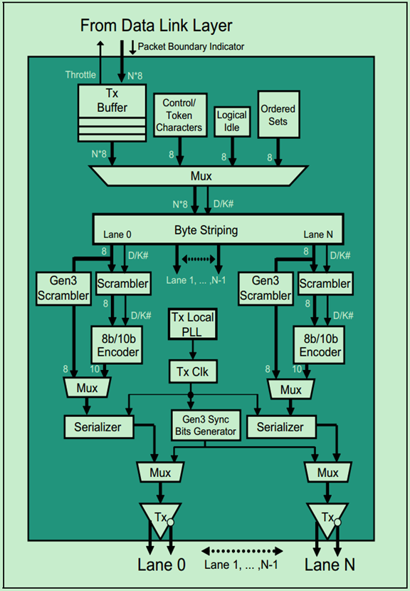
Before 8b/10b encoding, the Mux inserts some things into the data coming from the data link layer — control characters and data characters, used to mark packet boundaries or Ordered Sets. To tell those characters apart, the Mux attaches a D/K# bit to each one (Data or Kontrol).
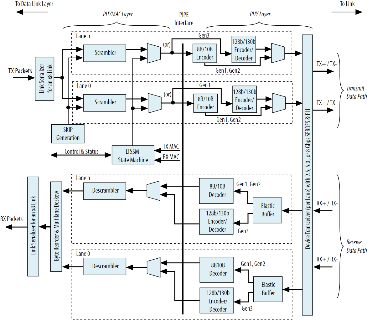
Note: the figure also includes some Gen3 implementation, but only Gen1 and Gen2 are covered here; Gen3 is not. If you are interested, read the Mindshare book or the PCIe Gen3 spec.
Byte striping distributes the parallel data from the Mux across the lanes according to a set of rules (detailed later). After that come the scrambler, 8b/10b encoding and the serialiser, and then the differential transmit pair.
The scrambler is XOR logic based on a pseudo-random code. Because the code is pseudo-random, the receiver can easily recover the data as long as transmitter and receiver use the same algorithm and the same seed. But if transmitter and receiver fall out of step for some reason, errors follow — which is why the Gen1 and Gen2 scramblers are reset periodically.
Receiver:
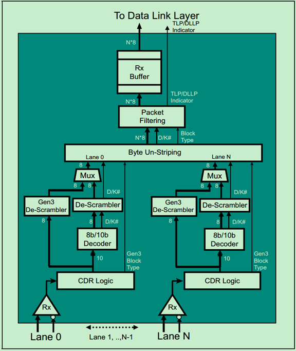
Because PCIe uses an embedded clock (by way of 8b/10b), the receiver’s first job on receiving the data stream is to recover the clock from it, which is what the CDR logic does. As the figure above shows, the receiver’s logic is basically the inverse of the transmitter’s, step for step. No need to go through it in detail.
The architecture as a whole: