Reading noteFrom adam-maj/tiny-gpu
Building a GPU by hand (1)
GPU
Nvidia has been surging for a year and GPUs are everywhere, but nobody has good material to learn from. There is a beginner’s GPU project on GitHub, tiny-gpu [https://github.com/adam-maj/tiny-gpu], that is well suited to studying. So I have picked apart its entire design, so that everyone can get a feel for how a GPU is designed and build one at home for fun. This write-up reads the code more or less line by line, so it need not sit gathering dust in your bookmarks.
Architecture
More CPU architectures are open today, but the low-level design of advanced GPUs is kept secret. tiny-gpu is the simplest GPU implementation there is, and it still covers how a GPU works. What this GPU is about is parallel computation (“hardware acceleration”), not graphics (“the rendering engine”).
Three things to look at:
- the architecture
- parallel processing
- memory (getting past the memory-bandwidth limit)
Architecture diagram
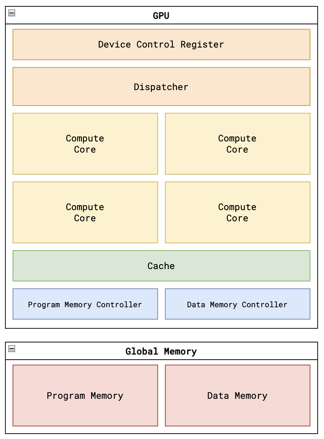
The overall architecture:
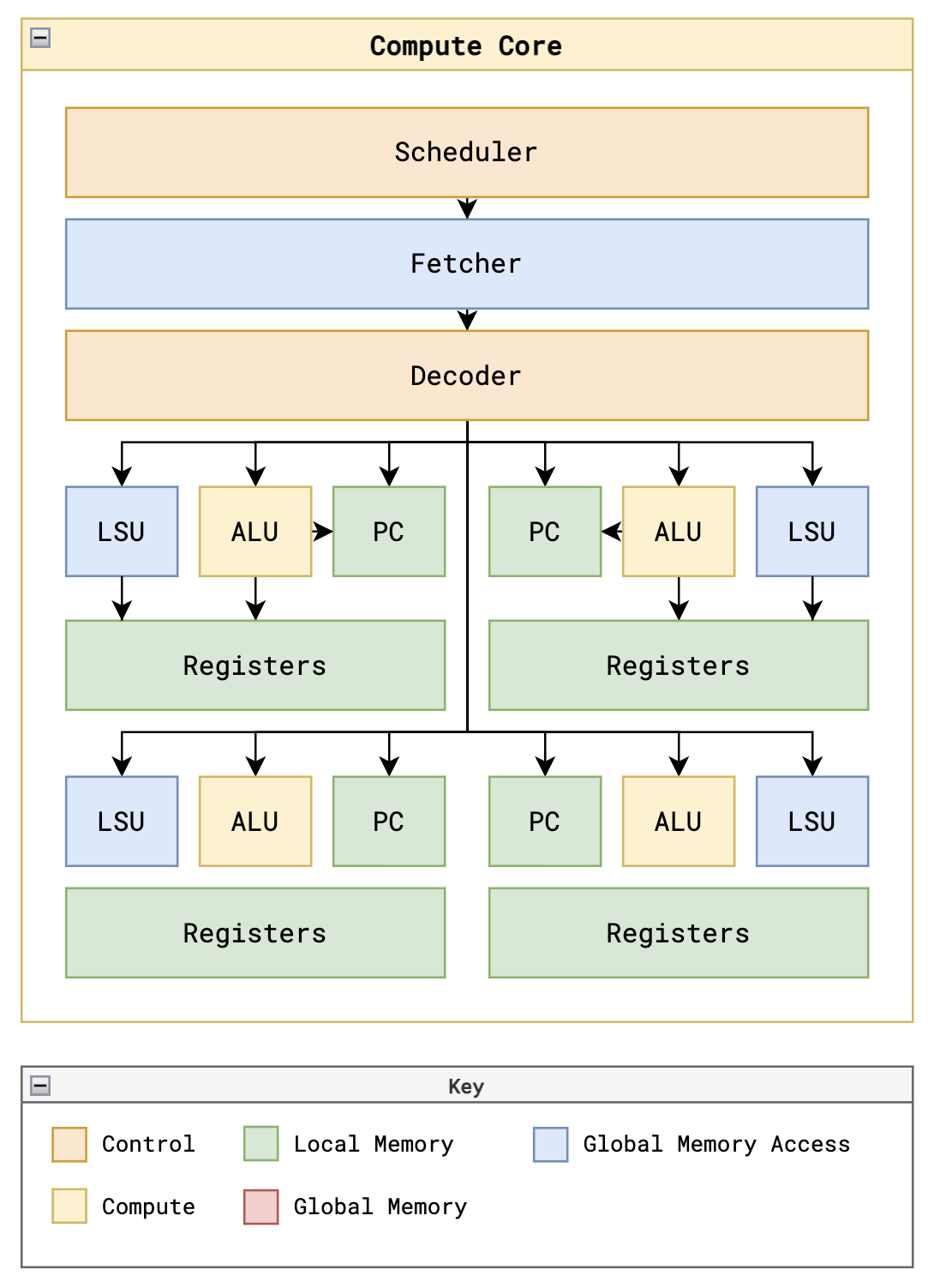
Inside a compute core:
How it runs, end to end
tiny-gpu executes one core at a time.
To start a core:
- Load global program memory with the kernel code (it is written in Python, using the cocotb co-simulation framework together with a makefile).
- Load whatever code is needed into data memory.
- Set how many threads to launch in the device control register.
- Pull the start signal high to run the kernel.
The GPU architecture contains:
- a device control register
- a dispatcher
- several compute cores
- memory controllers for data memory and program memory
- a cache
The data flow goes like this.
The .py files are the framework that runs the kernel in simulation, with a makefile as the script.
It really amounts to virtualised memory (because our GPU architecture only has memory controllers), plus the machine code for the program you want (add, subtract, multiply, divide, per the ISA), plus a clock. Think of it as the input and the output destination. Then there is the part that controls the running state of each stage and prints some logger files after the simulation.
Below, each part in detail, along with the Verilog.
Top level
See gpu.sv.
It declares a lot of variables, instantiates each part, and wires them together.
The part worth explaining here is the core instantiation.
// Compute Cores
genvar i;
generate
    for (i = 0; i < NUM_CORES; i = i + 1) begin : cores
        // EDA: We create separate signals here to pass to cores because of a requirement
        // by the OpenLane EDA flow (uses Verilog 2005) that prevents slicing the top-level signals
        reg [THREADS_PER_BLOCK-1:0] core_lsu_read_valid; // one hot
        reg [DATA_MEM_ADDR_BITS-1:0] core_lsu_read_address [THREADS_PER_BLOCK-1:0];
        reg [THREADS_PER_BLOCK-1:0] core_lsu_read_ready;
        reg [DATA_MEM_DATA_BITS-1:0] core_lsu_read_data [THREADS_PER_BLOCK-1:0];
        reg [THREADS_PER_BLOCK-1:0] core_lsu_write_valid;
        reg [DATA_MEM_ADDR_BITS-1:0] core_lsu_write_address [THREADS_PER_BLOCK-1:0];
        reg [DATA_MEM_DATA_BITS-1:0] core_lsu_write_data [THREADS_PER_BLOCK-1:0];
        reg [THREADS_PER_BLOCK-1:0] core_lsu_write_ready;

        // Pass through signals between LSUs and data memory controller
        // Load/Store Unit
        genvar j;
        for (j = 0; j < THREADS_PER_BLOCK; j = j + 1) begin
            localparam lsu_index = i * THREADS_PER_BLOCK + j;
            always @(posedge clk) begin
                lsu_read_valid[lsu_index] <= core_lsu_read_valid[j];
                lsu_read_address[lsu_index] <= core_lsu_read_address[j];

                lsu_write_valid[lsu_index] <= core_lsu_write_valid[j];
                lsu_write_address[lsu_index] <= core_lsu_write_address[j];
                lsu_write_data[lsu_index] <= core_lsu_write_data[j];

                core_lsu_read_ready[j] <= lsu_read_ready[lsu_index];
                core_lsu_read_data[j] <= lsu_read_data[lsu_index];
                core_lsu_write_ready[j] <= lsu_write_ready[lsu_index];
            end
        end

        // Compute Core
        core #(
            .DATA_MEM_ADDR_BITS(DATA_MEM_ADDR_BITS),
            .DATA_MEM_DATA_BITS(DATA_MEM_DATA_BITS),
            .PROGRAM_MEM_ADDR_BITS(PROGRAM_MEM_ADDR_BITS),
            .PROGRAM_MEM_DATA_BITS(PROGRAM_MEM_DATA_BITS),
            .THREADS_PER_BLOCK(THREADS_PER_BLOCK),
        ) core_instance (
            .clk(clk),
            .reset(core_reset[i]),
            .start(core_start[i]),
            .done(core_done[i]),
            .block_id(core_block_id[i]),
            .thread_count(core_thread_count[i]),

            .program_mem_read_valid(fetcher_read_valid[i]),
            .program_mem_read_address(fetcher_read_address[i]),
            .program_mem_read_ready(fetcher_read_ready[i]),
            .program_mem_read_data(fetcher_read_data[i]),

            .data_mem_read_valid(core_lsu_read_valid),
            .data_mem_read_address(core_lsu_read_address),
            .data_mem_read_ready(core_lsu_read_ready),
            .data_mem_read_data(core_lsu_read_data),
            .data_mem_write_valid(core_lsu_write_valid),
            .data_mem_write_address(core_lsu_write_address),
            .data_mem_write_data(core_lsu_write_data),
            .data_mem_write_ready(core_lsu_write_ready)
        );
    end
endgenerate
This uses generate, and the count is yours to set. The generate block does use a for loop, and the iteration count is not hard-coded, but when the hardware is inferred it elaborates against the core count actually defined and produces a real netlist.
In the core instantiation: our GPU has several cores, and each core has several threads. So, a simple double loop.
LSU is the load/store unit. Each thread has its own LSU, and localparam lsu_index = i * THREADS_PER_BLOCK + j; is there because i is the core index and j is the thread index. Say there are 2 cores with 4 threads each.
In the first core:
core[0] thread[0] LSU[0]
core[0] thread[1] LSU[1]
core[0] thread[2] LSU[2]
core[0] thread[3] LSU[3]
The second core then needs fresh LSU indices, because there is only the one set of LSU signal channels:
i * THREADS_PER_BLOCK + j = 1 * 4 + 0 = 4
core[1] thread[0] LSU[4]
core[1] thread[1] LSU[5]
core[1] thread[2] LSU[6]
core[1] thread[3] LSU[7]
// Compute Cores
genvar i;
generate
for (i = 0; i < NUM_CORES; i = i + 1) begin : cores
     // EDA: We create separate signals here to pass to cores because of a requirement
     // by the OpenLane EDA flow (uses Verilog 2005) that prevents slicing the top-level signals
     reg [THREADS_PER_BLOCK-1:0] core_lsu_read_valid; // one hot
     reg [DATA_MEM_ADDR_BITS-1:0] core_lsu_read_address [THREADS_PER_BLOCK-1:0];
     reg [THREADS_PER_BLOCK-1:0] core_lsu_read_ready;
     reg [DATA_MEM_DATA_BITS-1:0] core_lsu_read_data [THREADS_PER_BLOCK-1:0];
     reg [THREADS_PER_BLOCK-1:0] core_lsu_write_valid;
     reg [DATA_MEM_ADDR_BITS-1:0] core_lsu_write_address [THREADS_PER_BLOCK-1:0];
     reg [DATA_MEM_DATA_BITS-1:0] core_lsu_write_data [THREADS_PER_BLOCK-1:0];
     reg [THREADS_PER_BLOCK-1:0] core_lsu_write_ready;
This first half has to declare some global variables. Why: they are reusable, they are what you slice signals out of, and they get every signal onto the same clock.
On slicing: take the valid signal. Per thread per core it is really only one bit, and here we use one-hot, so later, when connecting the core’s pins, each valid has to have its own bit pulled out — .program_mem_read_valid(fetcher_read_valid[i]),. That is the slice. Which is why the top-level signals cannot be passed straight in.
// Pass through signals between LSUs and data memory controller
// Load/Store Unit
genvar j;
for (j = 0; j < THREADS_PER_BLOCK; j = j + 1) begin
    localparam lsu_index = i * THREADS_PER_BLOCK + j;
    always @(posedge clk) begin
        lsu_read_valid[lsu_index] <= core_lsu_read_valid[j];
        lsu_read_address[lsu_index] <= core_lsu_read_address[j];

        lsu_write_valid[lsu_index] <= core_lsu_write_valid[j];
        lsu_write_address[lsu_index] <= core_lsu_write_address[j];
        lsu_write_data[lsu_index] <= core_lsu_write_data[j];

        core_lsu_read_ready[j] <= lsu_read_ready[lsu_index];
        core_lsu_read_data[j] <= lsu_read_data[lsu_index];
        core_lsu_write_ready[j] <= lsu_write_ready[lsu_index];
    end
end
This is just an always block lining those signals up to the clock.
After that it is pin-to-pin connections, and nothing more.