Reading noteSource not recorded
Skimming ASIC synthesis (1)
ASIC synthesis: foreword
I will be job-hunting soon, and with classes over and nothing much to do, I may as well read. This series is a quick read through the overall ASIC synthesis flow — the whole ASIC design flow, from concept to the chip’s tape-out. It is also built on Design Compiler, so what it offers is the practice you actually use at work rather than theory. The book has six chapters. What you get off the page is always shallow; hands-on is worth a lot.
Chapter 1: how you should design an ASIC
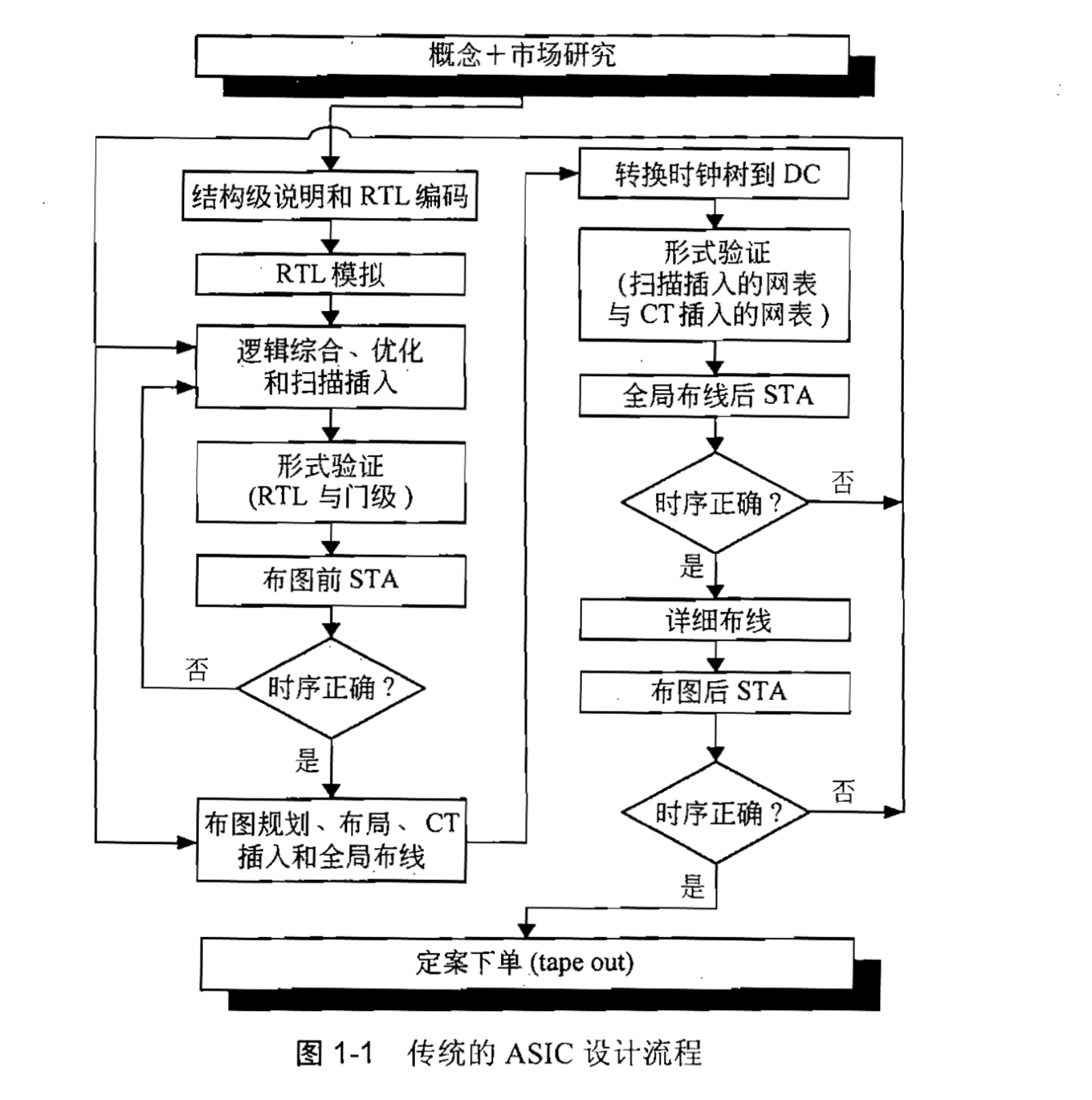
- Write the specification and the architecture — the architect’s job.
- RTL coding.
- Some designs have memory and need DFT memory BIST inserted.
- Verification.
- Environment setup: technology libraries and so on.
- Constrain and synthesise the design, with scan inserted (and optionally JTAG), using Design Compiler.
- Module-level STA with DC.
- Formal verification, comparing the RTL against the netlist.
- System-level STA with PrimeTime.
- Annotate the layout tool ahead of timing constraint.
- Initial layout partitioning for global routing.
- Clock tree into the netlist.
- Layout optimisation of the design with DC.
- Formal verification with Formality between the netlist and the netlist with the clock tree inserted.
- After global routing (step 11), extract estimated delays from the layout.
- Back-annotate the estimated delays into PrimeTime.
- STA using the estimated delays.
- Detailed placement of the design.
- Extract the actual delays of the detail-placed design.
- Back-annotate the actual delays into PrimeTime.
- STA using the real delays.
- Gate-level functional simulation (optional).
- After LVS and DRC, tape out.
There are three kinds of design: behavioural, RTL and structural. At the behavioural level you just write whatever it is you want to build. RTL is what gets converted into a netlist, so writing RTL is less writing than drawing a connection diagram of logic modules; you have to hold the digital design picture in your head.
Then comes dynamic simulation, to check the design’s function. Simulators today can all simulate behavioural and RTL, and sometimes the mapped gate-level design too. RTL simulation does not account for component or gate timing, so to minimise the difference between RTL simulation and post-synthesis gate-level simulation, delays are usually put in while coding RTL that has sequential elements.
People used to turn HDL into logic schematics by hand; now it is all done with synthesis tools. Synthesis is an iterative process. First you define timing constraints for every module in the design (they state how each signal relates to a particular module’s clock input). Besides the constraints, you also define a file for the synthesis environment, which states the technology library and the relevant information about DC’s use.
With the timing constraints applied, DC reads the RTL code and synthesises it to the structural level, producing a mapped gate-level netlist. For small module designs, DC has a built-in STA tool. If timing is not met, optimisation has to continue.
Designs today all fold in DFT logic so they can be tested. Design for testability.
Formal verification confirms a design by mathematical means, without regard to process factors (timing or physical effects). It is used to check the logic by comparison against a design. Unlike simulation, formal is about proving that two designs are logically equivalent in structure and function; simulation can only check the paths it sensitises, so it cannot possibly find the other problems that turn up. Formal verification is very, very fast next to simulation.
What formal verification verifies is the relationship between RTL and RTL, and between netlist and RTL. Extra features may get added and the design modified often, and when a feature is added on top of the RTL it may change logic function that was correct. There is also RTL against the scan-inserted gate level, to make sure the gate level has the same function. With simulation this takes too long (days, weeks); formal verification takes only hours. And there is gate level against gate level — the input and the output of layout — where the netlist with the clock tree inserted in between is a modification too, so logical equivalence has to be verified.
STA can analyse and report every critical path in detail, including fanout and the capacitive load of each net. STA is run on the gate-level netlist both before and after layout. Before layout, PrimeTime estimates net delays from the wire-load model that the technology library specifies; in the process, the timing constraints fed earlier to DC are also fed to PrimeTime, spelling out the relationship between inputs, outputs and the clock. If all the critical paths are acceptable, the result is a constraint file (.SDF), forward-annotated to the layout tool, which describes in detail the timing between each logic group the layout tool uses.
After layout, the actually extracted delays are back-annotated into PrimeTime to give a real delay calculation; these delays are all wire capacitance and interconnect RC delays.
STA is an iterative process too, tied closely to placement and routing. It takes many passes. It is tiring.
Floorplan and layout quality matter more than the routing itself. A good floorplan not only speeds up the final routing but also meets timing constraints better and reduces blocking. The constraint file is what drives timing-driven placement. A timing-driven placement approach lets the layout tool place units according to how timing-critical the paths between them are.
After unit layout, the clock tree is inserted into the design by the layout tool. Clock tree insertion is optional, depending on what the design needs and what the user prefers. The user can choose a traditional approach — for instance a fishbone/spine clock network, to cut total delay and clock skew. As process dimensions shrink and interconnect resistance rises (RC delay rises with it), the spine approach becomes hard to implement. I am putting the emphasis on the clock tree synthesis approach.